|
Telstar I - Dawn of a New Age
|
| Telstar I - Dawn of a New Age Copyright -
J. M. Early 1990 - from SMEC Vintage Electrics Volume #2 1990
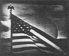
The first live television picture relayed from space.With
permission, Bell Laboratories RECORD. It was late afternoon of July 10, 1962. I was about two hundred miles south of Andover, in a motel near the University of New Hampshire at Durham, where the Solid State Device Research Conference was being held. It is hosted each year by a selected university. Much of the technology which made Telstar possible had been first published at this conference and at its predecessor, the Electron Device Research Conference, so that seeing the first Telstar broadcast while at the meeting seemed only right. My involvement with Telstar began after the AT&T-Bell Labs decision in 1960 that we could and would build and NASA would launch for AT&T a low orbit communications satellite. It was to be an all out job, a goal that must be achieved. It could be done, we knew that. We had to make it happen. Two major activities fell to my department. One was to design and test radiation-resistant high-efficiency solar cells and see that Western Electric built them to specification. We also had part of the job of insuring that the transistors selected were, to some degree at least, radiation resistant and, if necessary, seeing that the fabrication, test, and burn-in processes were modified to improve radiation resistance. Our tasks were only a small part of the total effort. Members of the Research Area, particularly Walter L. Brown, led the radiation studies work. At the same time, the system and circuit designers had the task of designing with adequate allowance for the predicted radiation-induced decrease of transistor gain and increase of junction leakage. Good radiation test data was essential. The key radiation resistance test facility had lethal potential. It was a strontium 90 source, as I remember, rated at a million curies. If it were in the open at ground level, a person 100 feet away would get a fatal dose in about 10 to 15 seconds. When in use it was shielded by thick lead walls, so no significant radiation could escape. When not in use, it was lowered into a lead-lined container, itself deep in a concreted below ground hole. This allowed the experimenters to place devices and test equipment around the operating position without hazard. A simple demonstration of the power of source was a slab of clear plastic, which had received, as I remember 100,000 rads. It had been yellowed, distorted, and cracked, grossly in all categories, without getting above room temperature. It intimidated. Tests invariably showed radiation susceptibilities in the devices planned for use. The question was "How much?" Mechanisms of degradation were postulated and changes in wafer fabrication were made to reduce the susceptibilities. Enough of the changes were effective to give major improvements in resistance to damage by radiation. Enough of the changes were ineffective to cause ulcers. There were those who thought this was much ado about very little. At that time, the presence of the van Allen radiation belts in the earth's magnetosphere was known. These belts were regions in which electrons and ions, created by ionizing radiation from outer space, orbited back and forth between north and south along the magnetic field of the earth, coming closest to earth above the two magnetic poles and being most distant from earth above the equator. The concentrations and energies of these particles were known roughly from satellite observations, ground data, and theory. The device engineering was such that the satellite should have had a life of many years despite this radiation. Unanticipated by the planners, and unknown to them, I believe, was that a hydrogen bomb was to be exploded in the upper atmosphere (the "Starfish Prime" test) on July 9, 1962. The Telstar launch was scheduled for the early hours of July 10, 1962. Both launches went per schedule. The bomb fired and Telstar worked. The bomb, however, gave rise to enormous numbers of high energy electrons and ions, a substantial fraction of which went into the van Allen belts. These swamped completely the normal van Allen belt populations, and caused noticeable radiation damage. Loss of control of the satellite repeater occurred first in August. Painstaking and brilliant analysis by the circuit and system engineers identified the specific point of failure and provided revised commands which effectively bypassed the failed circuit, thus restoring control and usefulness of the satellite until continuing radiation damage caused final failure a few weeks later. Sometime in the late summer or autumn of 1962, I encountered the Telstar project director, E. F. (Gene) O'Neill, in the Hunt Club room of the Hotel Suburban at Summit, N. J. near the Murray Hill Laboratories, I told him we were sorry we hadn't done better on the radiation resistance. In characteristic fashion, he put an arm around me, smiled widely and told me not to worry about, saying "Forget it! We had thirty-six risks that ranked higher than that!" He was delighted that we had all done so well. O'Neill would not have been so pleased if the transistors used in Telstar I had been as radiation sensitive as the first ones tested. During the development period, numerous tests were made. These led to changes in wafer processing, changes in transistor assembly and encapsulation, and changes in "burn-in" or conditioning procedures. The radiation test facility played a key role here, but units were also subjected to other types of ionizing radiation at university and government facilities all across the country. The solar cell design, led by Friedolf M. Smits, a native of Germany, was based in part on theoretical expectations of higher radiation resistance for N+ on P cells than for the P+ on N cells which had been the standard from the beginning of solar cells. Some experiments supporting this view had, I think, been done; where, I don't remember. The diffused N+ surface layer was thinner than any previously used in a diffused silicon device. This was to get and keep high efficiency in converting energy. The surface of the cell was to be coated with an oxide which would allow maximum transmission of light (anti-reflection coating) so as to have maximum solar energy reach the cell. Making electric contact to the very thin diffused layer posed new problems. The contact had to be of low resistance and therefore had to penetrate the thin layer of oxide which forms very rapidly whenever a silicon surface is exposed to oxygen. The contact could not be allowed to penetrate through the surface diffusion layer and thereby short-circuit the cell. Martin P. Lepselter, an exceptionally thorough and brilliantly creative engineer and metallurgist, solved this problem with a vacuum-deposited two-layer contact of titanium and silver. He chose titanium for two key properties, its affinity for oxygen and its complete miscibility with its own oxide. The first property caused it to reduce chemically the surface oxide on the silicon solar cells and thus reach the silicon. The second property guaranteed electrical conduction until the titanium contained a large proportion of oxygen. The silver gave good contact with the titanium, protected it from further oxidation easy soldering of contacts to the cells. The use of relatively high resistivity p-type silicon for the cell body also posed new problems in making electrical contact. Metals carry current by means of free or conduction electrons. A metal contact to p-silicon tends to create a Schottky barrier, a depletion region almost empty of mobile charges. To get the solar-generated current across such a layer would use a substantial fraction of the solar cell voltage and reduce its conversion efficiency sharply, thus requiring the use of much larger numbers of cells. This was not acceptable. K. D. Smith, as best I remember, proposed that contact be made by sand-blasting the back sides of the cells and making metallic contact to this surface. The sandblasting broke the single crystal structure and created a layer in which the valence band and the conduction band of the p-silicon were effectively connected to each other, short-circuited locally as it were. It wasn't a new approach, but many details had to be worked out. It wasn't an ideal answer but it resolved the impasse. That was what mattered. During the sand-blasting the front surface of the cell had to be protected from the grit. This didn't always work. K.D. Smith showed me one day a statistical study of the short-circuit current output of some 3000 cells exposed to an equivalent sunlight test. The currents were plotted on "probability paper", which transforms a perfect bell-shaped probability distribution (a Gaussian distribution) to a straight line. The plot was the straightest line I've ever seen for a large experiment, but there were sharp deviations in about the last 1% at each end, indicating unusual numbers of cells with excessively low or high currents. K. D. and I looked together at the offending cells and found that the low current cells typically had minor sand blast damage on the front face and that the high current cells had front face chemical stains which made substantial areas bluer than usual. The sand blast damage, which created a partial short circuit, was relatively easy to avoid, but, unhappily, we didn't get the bluer oxide under control in time to meet schedule. It increased solar transmission into the cell and gave higher electrical output. The project called for the best that was achievable to schedule. This led to designs which, even now, are remarkable. One foreseeable problem was, of course, enormous, very rapid, and repeated temperature changes. when the satellite was to be spinning in full sunlight with its axis at right angles to the sun's rays, its faces would go from sunlight to shadow many times a minute. If it was end on to the sun, one end would face the chill of outer space, the other would bake under the sun. When it went into the earth's shadow, over half the satellite would face outer space, and somewhat less than half would face the earth. Detailed thermal modeling made clear that temperature changes would be large and rapid. The obvious answer for the solar cell array design was to use materials compatible in thermal expansion and meeting radiation, strength, insulation, and assembly requirements. It was done. Rectangular ceramic slabs just over 2 cm wide were designed and shaped to support groups of the 1x2 cm solar cells. A transparent cover was provided for each cell, made of material with very low susceptibility to discoloration and loss of light transmission from the effects of the radiation environment. Metal rails were designed to attach to the sides of the ceramic cell support and to the ends of the transparent covers, themselves just over lx2 cm. The materials were a good thermal expansion match to silicon. It all went together and worked as designed. The ceramic was a fine grain, high density alumina. The cover material was colorless, melt-grown, single crystal aluminum oxide, sliced, polished to final thickness, and cut to size. This crystalline aluminum oxide is better known as white sapphire. The metal was platinum. This may seem "gilding the lily". Remember that a working satellite in orbit was the goal, not meetings defending the "economies" achieved in the design and building of a failure! That this first asynchronous low orbit satellite scheme
(hundreds of miles) was made obsolete by the development and placing of
extreme altitude synchronous orbit satellites (22,400
Transoceanic communication is a glorious and continuing chapter in human achievement, with trans-Atlantic service being the prototype for the other oceans. Until that splendid July 10th almost 30 years ago, the record read: first successful telegraph cable, 1866; first trans-Atlantic wireless telegraph transmission, 1901; first trans-Atlantic voice communication, 1927; first trans-Atlantic telephone cable, 1956. To have contributed to adding "first trans-Atlantic television transmission, 1962" to that list was, for me, and for many others, deeply satisfying. In truth, it made my day!
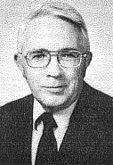
James M. Early was born (July 25, 1922) in Syracuse, New York, second of the nine children of Rhoda G. Early and the late Frank J. Early. He received the B.S. in Pulp and Paper Manufacturing in 1943 from the New York State College of Forestry (Syracuse). After army service at Ohio State University and the Manhattan Engineer District, Oak Ridge, Tenn., he returned to O.S.U. as a graduate student and instructor in Electrical Engineering. He received the M.S. (magnetron resonances) in 1948 and the Ph.D. (anisotropic dielectric waveguides) in 1951. He joined Bell Laboratories in September 1951. During his eighteen years at Bell, he created much of the design theory of bipolar transistors, discovered the effects of space-charge layer widening ("Early effect"), created the oscillator transistor for the first U.S. satellite, led development of solar cells and transistors for Telstar I, and led the development of sealed junction technology as part of Bell Lab's first major IC work, ending his Bell Labs service as Director of the Electron Device Laboratory at Allentown, Pa. He joined Fairchild in September 1969 as leader of their research and development work. Under his direction and often with his significant personal contributions, Fairchild Research Center created the isoplanar bipolar process and the prototype of the its isoplanar memory products, created the buried channel CCD imagers which have revolutionized low light level electronic imaging, created the prototypes of the 4000C series of 15 volt CMOS, created the 100K series of ECL, and contributed to the creation of FAST. His leadership brought Fairchild the first ion implanter in a merchant semiconductor manufacturing company (1970) and the first commercial electron beam mask-making machine (MEBES 1 - 1977). He became a technical adviser in mid-1983 and retired from Fairchild at the end of 1986. He is a fellow of IEEE (1958), a member of APS, AAAS, and Sigma XI. His IEEE service includes the Fellow Committee, ED Adcom, ED Transactions, IEEE PROCEEDINGS, and SPECTRUM. He is an IEEE representative on the Fritz Medal committee of the IEEE. He has published numerous technical papers and holds fourteen patents. He was associated with the Advisory Group on Electron Devices (ODDR&E) since 1962 to 1982 and was its chairman for four years. Jim and his wife, Mary Agnes, of 42 happy years live in Palo Alto, California. Their pastimes include duplicate bridge, bicycling, swimming, and reading.
|